- Home
-
Products
- Magnetic Ionic Liquid
-
Magnetic Beads
- Streptavidin Magnetic Beads
- Aldehyde Magnetic Beads
- Alkynyl Magnetic Beads
- Amino Magnetic Beads
- Avidin Magnetic Bead
- Azide Magnetic Beads
- Carboxyl Magnetic Beads
- DEAE Magnetic Beads
- Epoxy Magnetic Beads
- Heparin Magnetic Beads
- Hydroxyl Magnetic Beads
- NHS Magnetic Beads
- Phenyl Magnetic Beads
- Protein Magnetic Beads
- Silica Magnetic Beads
- Silicon Magnetic Beads
- Thiol Magnetic Beads
- Tosyl Magnetic Beads
- Magnetic Nanodispersion
- Ferrite Magnetic Nanopowder
- High-Purity Magnetic Nanomaterials
- Magnetic Polystyrene Microspheres
- Magnetic Bead Kit
- Magnetic Iron Oxide Nanocrystals
-
Magnetic Nanoparticles
- Amino-Functionalized Magnetic Nanoparticles
- Carboxyl-Functionalized Magnetic Nanoparticles
- Epoxy-Functionalized Magnetic Nanoparticles
- Hydrophobic Magnetic Nanoparticles
- IDA-Functionalized Magnetic Nanoparticles
- Magnetic Fe2O3 Nanoparticles
- Magnetic Fe3O4 Nanoparticles
- PEI Magnetic Nanoparticles
- PVA Magnetic Nanoparticles
- Silanol-Functionalized Magnetic Nanoparticles
- Urea Formaldehyde Magnetic Nanoparticles
- PAMAM Magnetic Nanoparticles
- Protein A Magnetic Nanoparticles
- Protein G Magnetic Nanoparticles
- Streptavidin Magnetic Nanoparticles
- Magnetic Silica Microspheres
-
Services
- Biomagnetic Material
- Magnetic Hydrogel Services
- Rare Earth Magnetic Materials Services
- Magnetic Ionic Liquid Services
- Magnetic Nanomaterials Services
- Magnetic Activated Carbon Service
- Molecular Magnetic Materials Services
- Magnetic Compounds Services
-
Custom Magnetic Beads Services
-
Biofunctionalized Magnetic Bead Services
- Magnetic Bead Protein Conjugation Services
- Magnetic Bead Antibody Conjugation Services
- Magnetic Bead Aptamer Conjugation Services
- Magnetic Bead Carbohydrate Conjugation Services
- Magnetic Bead Nucleic Acid Conjugation Services
- Magnetic Bead Drug Conjugation Services
- Magnetic Bead Enzyme Conjugation Services
- Magnetic Bead Metal Conjugation Services
- Magnetic Bead Multifunctional Composite Conjugation Services
- Magnetic Bean Affinity Tag Conjugation Services
- Magnetic Bead Affinity Ligand Conjugation Services
- Magnetic Bead Antigen Conjugation Services
- Magnetic Bead Fluorescent Material Conjugation Services
- Magnetic Bead Multiplex Conjugation Services
- Magnetic Bead Stimulus-Responsive Modification Services
- Magnetic Bead Enzyme-Responsive Modification Services
- Magnetic Bead Peptide Conjugation Services
- Magnetic Beads Glycolipid Conjugation Services
- Magnetic Beads Glycoprotein Conjugation Services
- Magnetic Bead Fluorescent Dye Conjugation Services
- Fluorescent-Magnetic Dual Functional Beads
- Magnetic Bead Conjugation Service for CRISPR Ribonucleoprotein
- Multiplexed Encoded Magnetic Beads Design Service
- Custom Magnetic Bead Synthesis
-
High-Performance Magnetic Beads Service
- Exosome Magnetic Bead Services
- High Affinity Magnetic Bead Service
- Immobilized Enzyme Magnetic Bead Services
- Low Non-Specific Adsorption Magnetic Bead Service
- Magnetic Bead Microfluidics Services
- Multimodal Magnetic Bead Services
- Protein Crystallization Magnetic Bead Services
- Ultra-Fast Responsive Magnetic Bead Services
- High-Stability Magnetic Bead Services
- Automated Magnetic Bead Processing Service
- Biocompatible Magnetic Bead Design Service
- Cell Sorting Magnetic Bead Design Service
- High Performance Magnetic Bead Characterization Service
- High-Sensitivity Biomarker Magnetic Bead Service
- Immune Enrichment Magnetic Bead Service
- Magnetic Bead GMP Production Service
- Molecular Diagnostics Magnetic Bead Service
- Nucleic Acid Extraction Magnetic Bead Design Service
- Protein Purification Magnetic Bead Design Service
- Protein Purification Magnetic Bead Service
-
Biofunctionalized Magnetic Bead Services
-
Nanomedicine Service
-
New Nanoparticle Design Services
- Complex Nanoparticle Design
- Nanoparticle Scalability Testing Service
- Polymer Nanoparticle Design Services
- Biobased Nanoparticles Design Service
- Gold Nanomaterials Design Service
- Metallic Nanoparticles Design Service
- Magnetite Nanoparticle Design Service
- Semiconductor Nanoparticles Design Service
- Titanium Dioxide Nanoparticles Design Service
- Metal Oxide Nanoparticles Design Service
- Silica Nanomaterials Design Service
- Carbon-Based Nanoparticles Design Service
- Nanomedicine CDMO Services
- Custom Nanoparticle Development and Manufacturing for Diagnostics
- Custom Nanoparticles Synthesis
- Nanoparticle Characterization Service
-
New Nanoparticle Design Services
-
Magnetic Beads Separation & Purification Services
- Antigen Sorting Magnetic Bead Service
- Clinical Sample Testing Magnetic Bead Service
- Environmental detection Magnetic Bead Service
- Food Testing Magnetic Bead Service
- Protein Sorting Magnetic Bead Service
- Serum Testing Magnetic Bead Service
- Virus Particle Enrichment Magnetic Bead Service
- Pollutant Detection Magnetic Bead Service
-
Magnetic Beads QC & Validation Services
- Magnetic Bead Activity Verification Service
- Magnetic Bead Adsorption Capacity Evaluation Service
- Magnetic Bead Binding Capacity Testing Service
- Magnetic Bead Biocompatibility Analysis Service
- Magnetic Bead Conjugation Efficiency Detection Service
- Magnetic Bead Consistency Validation
- Magnetic Bead Imaging Analysis Service
- Magnetic Bead Magnetic Response Speed Testing Service
- Magnetic Beads Particle Size Distribution Analysis Service
- Magnetic Bead Magnetic Detection Service
- Magnetic Bead Magnetic Strength Testing Service
- Magnetic Bead Morphology Analysis Service
- Magnetic Bead Stability Assessment Service
-
Magnetic Beads Application Development Services
- Magnetic Bead ELISA Platform Development Service
- Magnetic Bead Microfluidic Platform Development Service
- Molecular Diagnosis and Nucleic Acid Platform Development Services
- Nucleic Acid Probe Screening Magnetic Beads Service
- Magnetic Bead High-Throughput Drug Screening Platform Development
- Magnetic Bead Assisted Single-Cell Sorting Platform Development
- Magnetic Bead Based Environmental Pollutant Detection Platform Development
- Magnetic Bead Bubble Separation Platform Development
- Magnetic Bead Clinical Biochemical Index Detection Platform Development
- Magnetic Bead Coupled Vaccine Delivery System Platform Development
- Magnetic Bead Disease Marker Screening Platform Development
- Magnetic Bead Enhanced Chemiluminescence (ClLA) Detection Platform Development
- Magnetic Bead Environment Microbial Research Platform Development
- Magnetic Bead Food Microbial Detection Platform Development
- Magnetic Bead Gene Editing Verification Platform Development
- Magnetic Bead Heavy Metal Detection Platform Development
- Magnetic Bead Inflammatory Marker Detection Platform Development
- Magnetic Bead Liquid Biopsy Platform Development
- Magnetic Bead Pesticide Residue Detection Platform Development
- Magnetic Bead Stem Cell Differentiation Research Platform Development
- Magnetic Bead Stem Cell Screening Platform Development
- Magnetic Bead Tumor Single-Cell Sequencing Platform Development
- Magnetic Bead Virus Vector Purification Platform Development
- Magnetic Bead-Based Foodborne Pathogen Detection Platform Development
- Magnetic Bead Infectious Disease Diagnosis Platform Development
- Magnetic Bead-Based Western Blot Assistance Platform Development
- Amino Blocking Magnetic Bead Design Service
-
Advanced Magnetic Materials Services
- Custom Magnetic Carbon Material Services
-
Magnetic Ionic Liquids and Functional Compounds Service
- Magnetic Compounds Development Services
- Magnetic Ionic Liquid Technology Services
- Magnetic Ionic Liquid Bio-application Services
- Magnetic Ionic Liquid Characterization and Analysis Services
- Magnetic Ionic Liquid Customization Services
- Magnetic Ionic Liquid Formulation Optimization
- Magnetic Ionic Liquid Recycling and Regeneration Services
- Magnetic Ionic Liquid Separation Technology Development Services
- Magnetic Ionic Liquids and Catalysis Services
- Magnetic Ionic Liquid Formulation Optimization Services
- Magnetic Ionic Liquid Analytical Testing Services
- Custom Magnetic Nanoparticle Services
-
Rare Earth Magnetic Materials Development and Coating Services
- Custom Rare Earth Magnetic Material Formulation Services
- High-Performance Rare Earth Magnet Research Services
- Next-Generation Rare Earth Magnet Development Services
- Precision Rare Earth Magnetic Material Engineering
- Rare Earth Magnetic Composite Development Services
- Rare Earth Magnetic Material Coating Service
- Rare Earth Magnetic Materials Property Optimization Services
- Rare Earth Magnetic Materials Technology Services
- Specialty Rare Earth Magnetic Materials Design
- Sustainable Rare Earth Magnet Development Solutions
-
Magnetic Hydrogel and Intelligent Response System Services
- 3D Printing Magnetic Hydrogel Customization Services
- Antibacterial Magnetic Hydrogel Services
- Bio-Application Targeted Magnetic Hydrogel Solutions
- Biomedical Magnetic Hydrogels Services
- Biomedical-Grade Targeted Magnetic Hydrogel Platform Development
- Biotargeted Release Magnetic Hydrogel Services
- Custom Biotargeted Release Magnetic Hydrogel Services
- Custom Multifunctional Magnetic Hydrogel Services
- Drug Delivery Magnetic Hydrogel Development Services
- Enzyme-Responsive Magnetic Hydrogel Platform Development
- Gene Therapy Magnetic Hydrogel Services
- Intelligent Magnetic-Responsive Hydrogel Services
- Magnetic Hydrogel Performance Optimization Services
- Magnetic Hydrogel Synthesis Services
- Magnetic Nanocomposite Hydrogel Customization Services
- Magnetic-Responsive Hydrogel Formulation Design Services
- Microfluidic Magnetic Hydrogel Services
- PH Responsive Magnetic Hydrogel Platform Development
- Thermal Responsive Magnetic Hydrogel Platform Development
-
Magnetic Bead Labeling Technology Service
- Antigen Magnetic Beads Custom Labeling Service
- Antibody Purification Magnetic Bead Design Services
- High-Sensitivity Antibody Magnetic Bead Coating Service
- Antimicrobial Peptide (AMP) Screening Magnetic Bead Service
- Immunomagnetic Bead Oriented Labeling Service
- Capture Sequencing Magnetic Bead Design Service
- Magnetic Bead Biological Ligand Affinity Purification Labeling Service
- Chemiluminescence Magnetic Bead Design Service
- Magnetic Bead Probe Design and Validation Service
- Immunoassay Magnetic Bead Design Service
- Magnetic Bead Surface Carboxyl Activation Service
- Magnetic Bead Agar Modification Service
- Magnetic Beads Labeling Process Development Service
- Magnetic Bead Aldehyde Modification Services
- Multi-Omics Sample Pretreatment Magnetic Bead Labeling Service
- Magnetic Bead Amine Modification Service
- Nucleic Acid Probe Magnetic Bead Conjugation Service
- Magnetic Bead Epoxidation Modification Service
- Magnetic Bead Organic Solvent Resistant Modification Service
- Magnetic Bead Silicon Hydroxy Acid Modification Service
- Magnetic Bead-Based Glycan Enrichment Service
- Magnetic Bead-Based Glycoprotein Enrichment Service
- Magnetic Beads for Host Cell Protein (HCP) Removal Service
- Mitochondria Isolation Magnetic Beads Development
- Nanobody Magnetic Bead Design Services
- Phosphopeptide Enrichment Magnetic Bead Service
- RNA-Seq Magnetic Bead Design Service
- RT-PCR Amplification Magnetic Bead Design
- Solid Phase Extraction Magnetic Bead Development Service
- Thermal Contrast Imaging Magnetic Bead Design Service
- Vaccine Antigen Purification Magnetic Beads Design
- Anti-Biotin Magnetic Bead Development
-
Magnetic Bead Detection Service
- Functional Binding Assessment for Magnetic Beads
- Magnetic Bead Biological Stability Detection Service
- Magnetic Bead Chemical Stability Detection Service
- Magnetic Bead Density Quantification Service
- Magnetic Bead Magnetic Response Speed Detection Service
- Magnetic Bead Sterility Testing Service
- Magnetic Bead Surface Topography & Smoothness Detection Service
- Magnetic Magnetization Detection Service
- Magnetic Size & Distribution Detection Service
- Magnetic Bead Formulation Service
- Magnetic-Bead Based OEM Solutions
- Support
- About Us
- Contact Us

- Magnetic Compounds Services
- Molecular Magnetic Materials Services
- Magnetic Activated Carbon Service
- Magnetic Nanomaterials Services
- Magnetic Ionic Liquid Services
- Rare Earth Magnetic Materials Services
- Magnetic Hydrogel Services
- Biomagnetic Material
-
Custom Magnetic Beads Services
-
Biofunctionalized Magnetic Bead Services
- Magnetic Bead Protein Conjugation Services
- Magnetic Bead Antibody Conjugation Services
- Magnetic Bead Aptamer Conjugation Services
- Magnetic Bead Carbohydrate Conjugation Services
- Magnetic Bead Nucleic Acid Conjugation Services
- Magnetic Bead Drug Conjugation Services
- Magnetic Bead Enzyme Conjugation Services
- Magnetic Bead Metal Conjugation Services
- Magnetic Bead Multifunctional Composite Conjugation Services
- Magnetic Bean Affinity Tag Conjugation Services
- Magnetic Bead Affinity Ligand Conjugation Services
- Magnetic Bead Antigen Conjugation Services
- Magnetic Bead Fluorescent Material Conjugation Services
- Magnetic Bead Multiplex Conjugation Services
- Magnetic Bead Stimulus-Responsive Modification Services
- Magnetic Bead Enzyme-Responsive Modification Services
- Magnetic Bead Peptide Conjugation Services
- Magnetic Beads Glycolipid Conjugation Services
- Magnetic Beads Glycoprotein Conjugation Services
- Magnetic Bead Fluorescent Dye Conjugation Services
- Fluorescent-Magnetic Dual Functional Beads
- Magnetic Bead Conjugation Service for CRISPR Ribonucleoprotein
- Multiplexed Encoded Magnetic Beads Design Service
- Custom Magnetic Bead Synthesis
-
High-Performance Magnetic Beads Service
- Exosome Magnetic Bead Services
- High Affinity Magnetic Bead Service
- Immobilized Enzyme Magnetic Bead Services
- Low Non-Specific Adsorption Magnetic Bead Service
- Magnetic Bead Microfluidics Services
- Multimodal Magnetic Bead Services
- Protein Crystallization Magnetic Bead Services
- Ultra-Fast Responsive Magnetic Bead Services
- High-Stability Magnetic Bead Services
- Automated Magnetic Bead Processing Service
- Biocompatible Magnetic Bead Design Service
- Cell Sorting Magnetic Bead Design Service
- High Performance Magnetic Bead Characterization Service
- High-Sensitivity Biomarker Magnetic Bead Service
- Immune Enrichment Magnetic Bead Service
- Magnetic Bead GMP Production Service
- Molecular Diagnostics Magnetic Bead Service
- Nucleic Acid Extraction Magnetic Bead Design Service
- Protein Purification Magnetic Bead Design Service
- Protein Purification Magnetic Bead Service
-
Biofunctionalized Magnetic Bead Services
-
Nanomedicine Service
- Nanomedicine CDMO Services
- Custom Nanoparticle Development and Manufacturing for Diagnostics
- Custom Nanoparticles Synthesis
- Nanoparticle Characterization Service
-
New Nanoparticle Design Services
- Complex Nanoparticle Design
- Nanoparticle Scalability Testing Service
- Polymer Nanoparticle Design Services
- Biobased Nanoparticles Design Service
- Gold Nanomaterials Design Service
- Metallic Nanoparticles Design Service
- Magnetite Nanoparticle Design Service
- Semiconductor Nanoparticles Design Service
- Titanium Dioxide Nanoparticles Design Service
- Metal Oxide Nanoparticles Design Service
- Silica Nanomaterials Design Service
- Carbon-Based Nanoparticles Design Service
-
Magnetic Beads Separation & Purification Services
- Antigen Sorting Magnetic Bead Service
- Clinical Sample Testing Magnetic Bead Service
- Environmental detection Magnetic Bead Service
- Food Testing Magnetic Bead Service
- Protein Sorting Magnetic Bead Service
- Serum Testing Magnetic Bead Service
- Virus Particle Enrichment Magnetic Bead Service
- Pollutant Detection Magnetic Bead Service
-
Magnetic Beads QC & Validation Services
- Magnetic Bead Activity Verification Service
- Magnetic Bead Adsorption Capacity Evaluation Service
- Magnetic Bead Binding Capacity Testing Service
- Magnetic Bead Biocompatibility Analysis Service
- Magnetic Bead Conjugation Efficiency Detection Service
- Magnetic Bead Consistency Validation
- Magnetic Bead Imaging Analysis Service
- Magnetic Bead Magnetic Response Speed Testing Service
- Magnetic Beads Particle Size Distribution Analysis Service
- Magnetic Bead Magnetic Detection Service
- Magnetic Bead Magnetic Strength Testing Service
- Magnetic Bead Morphology Analysis Service
- Magnetic Bead Stability Assessment Service
-
Magnetic Beads Application Development Services
- Magnetic Bead ELISA Platform Development Service
- Magnetic Bead Microfluidic Platform Development Service
- Molecular Diagnosis and Nucleic Acid Platform Development Services
- Nucleic Acid Probe Screening Magnetic Beads Service
-
Magnetic Bead High-Throughput Drug Screening Platform Development
- Magnetic Bead Antibody Drug Screening Platform Development
- Magnetic Bead Biopharmaceutical Drug Screening Platform Development
- Magnetic Bead Cancer Early Screening Platform Development
- Magnetic Bead Cell Therapy Drug Screening Platform Development
- Magnetic Bead Microbial Drug Screening Platform Development
- Magnetic Bead Nucleic Acid Drug Screening Platform Development
- Magnetic Bead Oligosaccharides Drug Screening Platform Development
- Magnetic Bead Peptide Drug Screening Platform Development
- Magnetic Bead Plant Molecular Breeding Platform Development
- Magnetic Bead Protein Drug Screening Platform Development
- Magnetic Bead Radiopharmaceutical Screening Platform Development
- Magnetic Bead Small Molecule Drug Screening Platform Development
- Magnetic Bead Targeted Drug Screening Platform Development
- Magnetic Bead Assisted Single-Cell Sorting Platform Development
- Magnetic Bead Based Environmental Pollutant Detection Platform Development
- Magnetic Bead Bubble Separation Platform Development
- Magnetic Bead Clinical Biochemical Index Detection Platform Development
- Magnetic Bead Coupled Vaccine Delivery System Platform Development
- Magnetic Bead Disease Marker Screening Platform Development
- Magnetic Bead Enhanced Chemiluminescence (ClLA) Detection Platform Development
- Magnetic Bead Environment Microbial Research Platform Development
- Magnetic Bead Food Microbial Detection Platform Development
- Magnetic Bead Gene Editing Verification Platform Development
- Magnetic Bead Heavy Metal Detection Platform Development
- Magnetic Bead Inflammatory Marker Detection Platform Development
- Magnetic Bead Liquid Biopsy Platform Development
- Magnetic Bead Pesticide Residue Detection Platform Development
- Magnetic Bead Stem Cell Differentiation Research Platform Development
- Magnetic Bead Stem Cell Screening Platform Development
- Magnetic Bead Tumor Single-Cell Sequencing Platform Development
- Magnetic Bead Virus Vector Purification Platform Development
- Magnetic Bead-Based Foodborne Pathogen Detection Platform Development
- Magnetic Bead Infectious Disease Diagnosis Platform Development
- Magnetic Bead-Based Western Blot Assistance Platform Development
- Amino Blocking Magnetic Bead Design Service
-
Advanced Magnetic Materials Services
- Custom Magnetic Carbon Material Services
-
Magnetic Ionic Liquids and Functional Compounds Service
- Magnetic Compounds Development Services
- Magnetic Ionic Liquid Technology Services
- Magnetic Ionic Liquid Bio-application Services
- Magnetic Ionic Liquid Characterization and Analysis Services
- Magnetic Ionic Liquid Customization Services
- Magnetic Ionic Liquid Formulation Optimization
- Magnetic Ionic Liquid Recycling and Regeneration Services
- Magnetic Ionic Liquid Separation Technology Development Services
- Magnetic Ionic Liquids and Catalysis Services
- Magnetic Ionic Liquid Formulation Optimization Services
- Magnetic Ionic Liquid Analytical Testing Services
- Custom Magnetic Nanoparticle Services
-
Rare Earth Magnetic Materials Development and Coating Services
- Custom Rare Earth Magnetic Material Formulation Services
- High-Performance Rare Earth Magnet Research Services
- Next-Generation Rare Earth Magnet Development Services
- Precision Rare Earth Magnetic Material Engineering
- Rare Earth Magnetic Composite Development Services
- Rare Earth Magnetic Material Coating Service
- Rare Earth Magnetic Materials Property Optimization Services
- Rare Earth Magnetic Materials Technology Services
- Specialty Rare Earth Magnetic Materials Design
- Sustainable Rare Earth Magnet Development Solutions
-
Magnetic Hydrogel and Intelligent Response System Services
- 3D Printing Magnetic Hydrogel Customization Services
- Antibacterial Magnetic Hydrogel Services
- Bio-Application Targeted Magnetic Hydrogel Solutions
- Biomedical Magnetic Hydrogels Services
- Biomedical-Grade Targeted Magnetic Hydrogel Platform Development
- Biotargeted Release Magnetic Hydrogel Services
- Custom Biotargeted Release Magnetic Hydrogel Services
- Custom Multifunctional Magnetic Hydrogel Services
- Drug Delivery Magnetic Hydrogel Development Services
- Enzyme-Responsive Magnetic Hydrogel Platform Development
- Gene Therapy Magnetic Hydrogel Services
- Intelligent Magnetic-Responsive Hydrogel Services
- Magnetic Hydrogel Performance Optimization Services
- Magnetic Hydrogel Synthesis Services
- Magnetic Nanocomposite Hydrogel Customization Services
- Magnetic-Responsive Hydrogel Formulation Design Services
- Microfluidic Magnetic Hydrogel Services
- PH Responsive Magnetic Hydrogel Platform Development
- Thermal Responsive Magnetic Hydrogel Platform Development
-
Magnetic Bead Labeling Technology Service
- Antigen Magnetic Beads Custom Labeling Service
- High-Sensitivity Antibody Magnetic Bead Coating Service
- Immunomagnetic Bead Oriented Labeling Service
- Magnetic Bead Biological Ligand Affinity Purification Labeling Service
- Magnetic Bead Probe Design and Validation Service
- Magnetic Bead Surface Carboxyl Activation Service
- Magnetic Beads Labeling Process Development Service
- Multi-Omics Sample Pretreatment Magnetic Bead Labeling Service
- Nucleic Acid Probe Magnetic Bead Conjugation Service
- Antibody Purification Magnetic Bead Design Services
- Antimicrobial Peptide (AMP) Screening Magnetic Bead Service
- Capture Sequencing Magnetic Bead Design Service
- Chemiluminescence Magnetic Bead Design Service
- Immunoassay Magnetic Bead Design Service
- Magnetic Bead Agar Modification Service
- Magnetic Bead Aldehyde Modification Services
- Magnetic Bead Amine Modification Service
- Magnetic Bead Epoxidation Modification Service
- Magnetic Bead Organic Solvent Resistant Modification Service
- Magnetic Bead Silicon Hydroxy Acid Modification Service
- Magnetic Bead-Based Glycan Enrichment Service
- Magnetic Bead-Based Glycoprotein Enrichment Service
- Magnetic Beads for Host Cell Protein (HCP) Removal Service
- Mitochondria Isolation Magnetic Beads Development
- Nanobody Magnetic Bead Design Services
- Phosphopeptide Enrichment Magnetic Bead Service
- RNA-Seq Magnetic Bead Design Service
- RT-PCR Amplification Magnetic Bead Design
- Solid Phase Extraction Magnetic Bead Development Service
- Thermal Contrast Imaging Magnetic Bead Design Service
- Vaccine Antigen Purification Magnetic Beads Design
- Anti-Biotin Magnetic Bead Development
-
Magnetic Bead Detection Service
- Functional Binding Assessment for Magnetic Beads
- Magnetic Bead Biological Stability Detection Service
- Magnetic Bead Chemical Stability Detection Service
- Magnetic Bead Density Quantification Service
- Magnetic Bead Magnetic Response Speed Detection Service
- Magnetic Bead Sterility Testing Service
- Magnetic Bead Surface Topography & Smoothness Detection Service
- Magnetic Magnetization Detection Service
- Magnetic Size & Distribution Detection Service
- Magnetic Bead Formulation Service
- Magnetic-Bead Based OEM Solutions
Semiconductor Nanoparticles Design Service
CD Bioparticles is a leading provider of innovative and customized solutions in the field of nanotechnology. We are proud to provide our professional semiconductor nanoparticle design services, which is a comprehensive platform for developing and optimizing high-quality semiconductor nanocrystals. These materials are commonly referred to as quantum dots (QDs) and are at the forefront of modern technology due to their unique size dependent optical and electronic properties. From quantum computing and advanced displays to biomedical imaging and solar energy, semiconductor nanoparticles are revolutionizing numerous industries. Our service aims to help you leverage this potential by providing tailored materials to meet your specific research or commercial application needs.
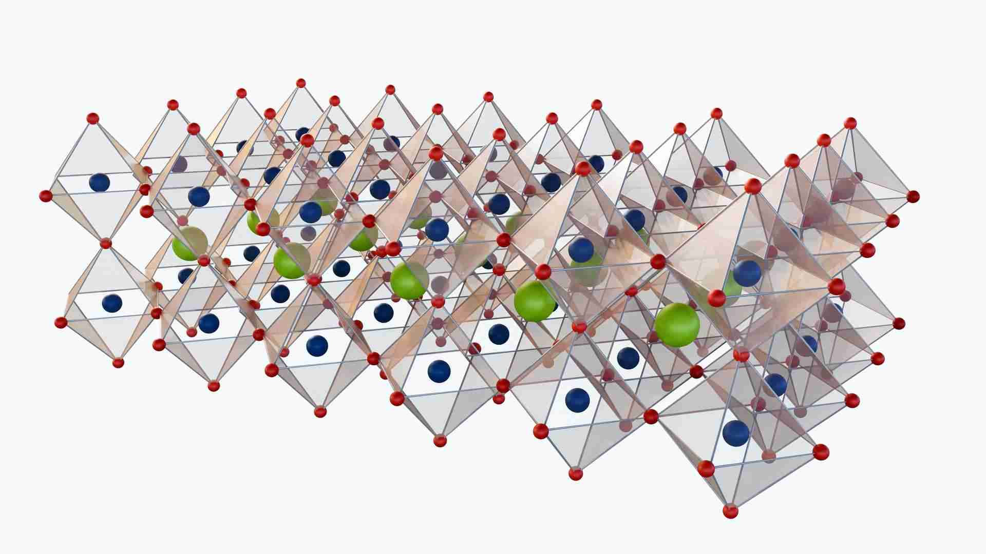 Figure 1. Semiconductor Nanoparticles Design Service.
The Power of Semiconductor Nanoparticles
Semiconductor nanoparticles are a type of material that exhibits quantum confinement phenomena. When their size decreases to the nanoscale, their electronic structure changes, resulting in size tunable properties. This means that by simply changing the size of nanoparticles, we can precisely control their optical and electronic behavior. The key attributes include:
Our Services
Our services leverage these advantages to provide you with materials that are not only powerful but also have excellent performance.
Material Composition
We offer a diverse range of semiconductor materials to suit various applications, including:
Size and Shape Control
The optoelectronic properties of semiconductor nanoparticles are strongly dependent on size and morphology, which we precisely control:
Surface Functionalization
Surface modification is critical for optimizing dispersion, biocompatibility, and device integration:
Optical and Electronic Property Tuning
We tailor key optoelectronic properties to match application requirements:
Technical Expertise and Comprehensive Methods
CD Bioparticles uses the most advanced synthesis technology to produce high-quality semiconductor nanoparticles:
Our Advantages

Customization Flexibility
From heavy-metal-free formulations to complex core-shell structures, we offer unparalleled flexibility to meet unique application demands.

Specialized Expertise
Our team includes materials scientists and engineers with extensive experience in semiconductor nanocrystal synthesis.

Regulatory Support
Assistance with compliance documentation for diverse industries, including electronics, healthcare, and energy.
Specific Application Expertise
Our semiconductor nanoparticle design services are tailored for a wide range of applications:
Workflow
Requirements Gathering
Design and Proposal
Conjugation
Quality Control
Delivery
Summary
Choosing CD Bioparticles for your semiconductor nanoparticle needs means partnering with a team of leading experts who are dedicated to your project's success. Our commitment to quality, innovation, and customer satisfaction sets us apart. With our flexible service model, state-of-the-art technology, and deep scientific expertise, we are uniquely positioned to help you push the boundaries of what is possible with semiconductor nanoparticles.